How to Achieve Precision Printing on Sapphire Crystals

How to Achieve Precision Printing on Sapphire Crystals

A Solution to the Problem of Inaccurately Identifying and Positioning the Substrate During Batch Printing of Outer Surface with a Alignment Accuracy of ± 0.01mm on Sapphire Crystals
    As an important technical crystal,Sapphire crystal is widely used in various fields such as infrared window materials,  substrates in microelectronics, laser substrates, optical components, and other applications.
    In March 2015, a customer inquired whether our screen printer could print a layer of resistance paste on the circular surface of sapphire crystals, with a alignment accuracy of ± 0.01mm.This is a very easy thing to achieve for our screen printer. So we proposed that the customer provide samples and conduct face-to-face communication.
    After the customer provided the samples, we found a problem: the sapphire crystal is transparent and colorless, and it is difficult to ensure the consistency of all product printing positions during mass production solely by mechanical alignment. SO we organized our company's technical engineers to discuss this critical issue and conducted multiple demonstrations and tests on our proposed solution through our thick film printing laboratory. 
   Three days later, we proposed two solutions to the customer: first,we will apply the CCD visual alignment system to achieve the goal of automatic alignment and precision printing. Second,Due to the lack of clear reference points in sapphire crystals, it is difficult for CCD to accurately identify and locate them, so we need to use a special MARK point recognition and positioning method.
    After internal evaluation, the customer unanimously approved our solution. Two months later, the equipment was delivered and successfully passed customer testing and acceptance.
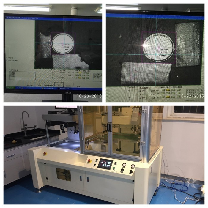
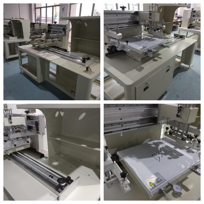
Matching Screen Printer
IC-200A-CCD Screen Printer
Maximum printing size: 200mmx200mm The printing accuracy: ± 5um The screen printer can be used for precision screen printing of ceramic substrates, electronic components,sensor ,PCB boards and other fields. It is equipped with CCD automatic visual alignment to reduce manual feeding errors.
View More
IC-200A-LTCC Screen Printer
Maximum printing size: 130mmx130mm The printing accuracy: ± 5um This is the special screen printer for Production of Multilayer circuit Components such as LTCC,HTCC,MLCC, fuel cell,solar cell,etc. The platform is equipped with a special roll paper platform, effectively preventing cross contamination during printing.
View More
IC-150B-CCD Screen Printer
Maximum printing size: 150mmx150mm The printing accuracy: ± 5um The screen printer can be used for precision screen printing of ceramic substrates, electronic components,sensor, PCB boards and other fields. It is equipped with CCD automatic visual alignment to reduce manual feeding errors.
View More
IC-250B-CCD Screen Printer
Maximum printing size: 250mmx250mm The printing accuracy: ± 5um The screen printer can be used for precision screen printing of ceramic substrates, electronic components, ,PCB boards and other fields. It is equipped with CCD automatic visual alignment to reduce manual feeding errors. The IC-250B screen printer is an upgraded version of the IC-250A, with the main difference being that some precision accessories have different brands and the same functions
View More
Your Name*
Email*
Printing Materials
Choose your substrate material
Ceramics
Metals
Thin Films
Wafers
Glass
Other Materials
Printing Area*
Choose your products printing area
≤150x150mm
≤250x250mm
≤400x400mm
≤600x600mm
>600x600mm
Process requirements