
1.What is a Ceramic Antenna?
A ceramic antenna is a miniature resonant antenna made with a high-permittivity ceramic dielectric as its substrate. High-permittivity ceramics can compress the guided wavelength within the medium, significantly reducing the antenna size while maintaining positioning and communication performance — perfectly matching the design trends of miniaturization and slimness in electronic products.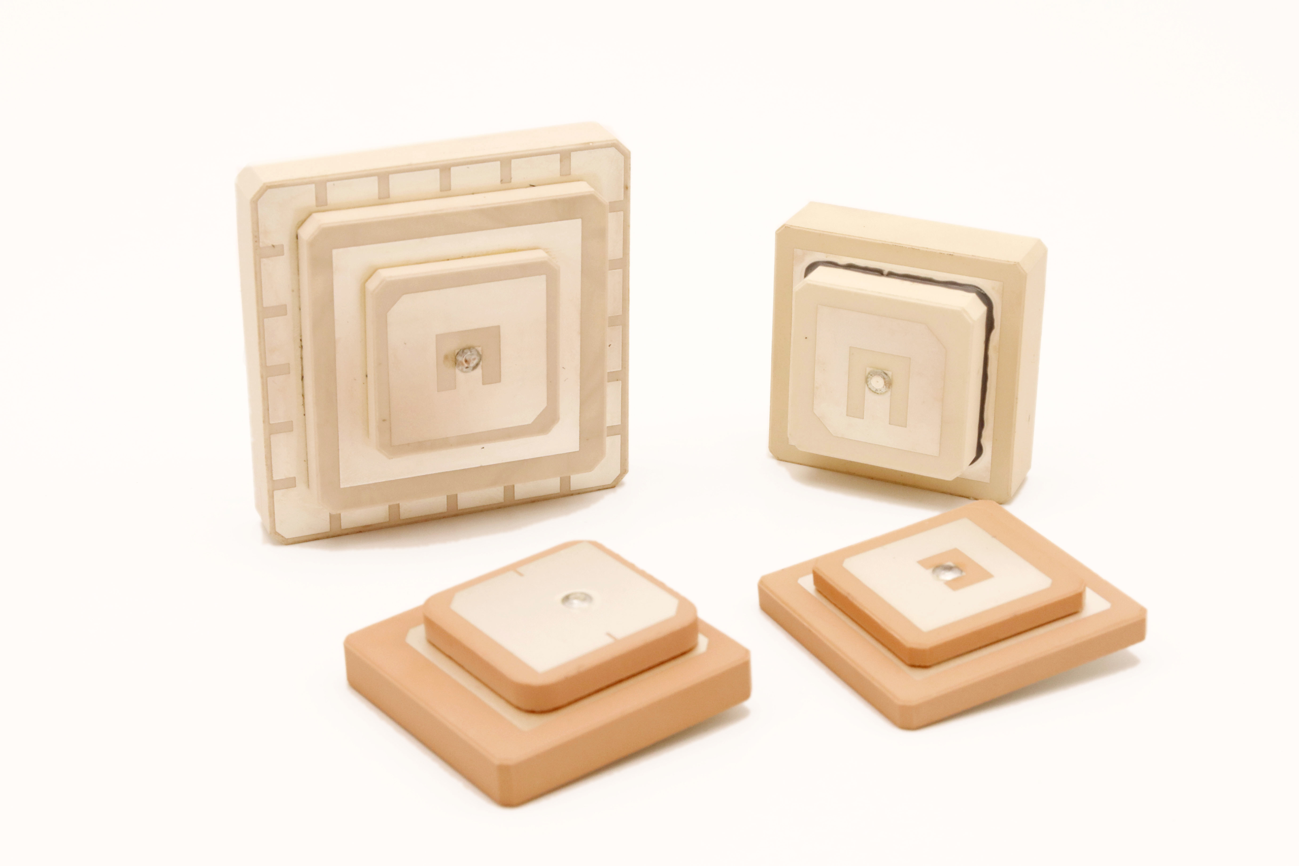
Ceramic Antenna | Source: Songyuan Electronics
By manufacturing process, they are divided into bulk ceramic antennas and LTCC (Low-Temperature Co-fired Ceramic) multilayer ceramic antennas: bulk ceramic antennas are made by forming conductive circuits on the surface of a sintered ceramic substrate, while LTCC antennas embed multilayer conductor circuits between ceramic layers, offering higher integration and a more compact structure. Both types require the fabrication of high-precision conductive circuits on ceramic substrates, which is precisely a core application scenario for thick film printing.
2.How Are Conductive Patterns Printed onto Ceramics?
The ability of a ceramic antenna to transmit and receive wireless signals does not come from the ceramic itself, but from the conductive patterns printed on the ceramic surface. These patterns are typically made of silver paste or palladium-silver paste, precisely transferred onto the ceramic substrate through thick film screen printing, and then sintered to form a stable and reliable conductive layer.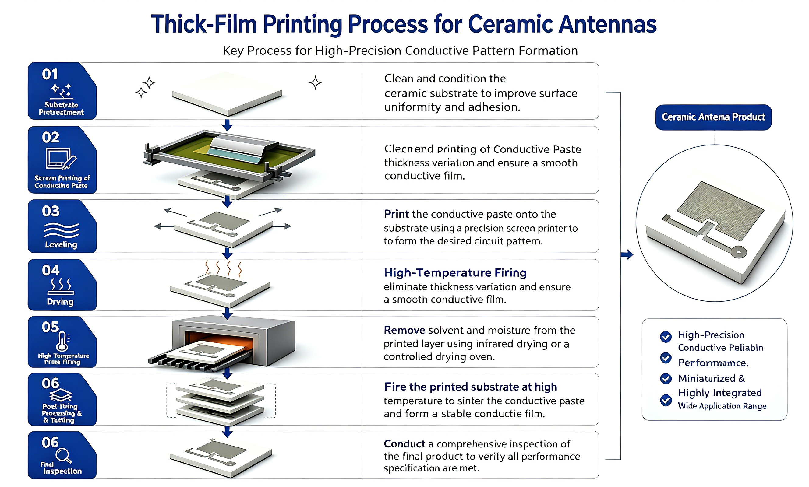
Ceramic Antenna Screen Printing Process Flowchart
Before printing, the ceramic substrate must undergo a cleaning process to ensure the conductive paste adheres firmly. Subsequently, the conductive paste is printed through a screen mesh into functional patterns such as radiation patches, feed points, and ground layers. After processes including leveling, drying, and sintering, a metal layer with good conductivity and reliability is ultimately formed.
For LTCC multilayer ceramic antennas, it is also necessary to complete multilayer conductor circuit printing and layer-to-layer registration to meet the manufacturing requirements of higher integration and more complex structures.
Thick film screen printing not only accomplishes the fabrication of conductive patterns but also directly affects the performance, consistency, and long-term reliability of ceramic antennas.
3.Why Does Printing Accuracy Determine Ceramic Antenna Performance?
Many people assume that screen printing is simply about applying paste onto a substrate. However, in the field of ceramic substrates, the real challenge lies in precision patterning manufacturing.
Key Control Points:
●Clear pattern edges — avoiding burrs and jagged edges to reduce high-frequency signal loss.
●Stable line width and spacing — ensuring consistent impedance and improving antenna performance.
●Uniform film thickness — contributing to stable conductive performance.
●Accurate multilayer registration — meeting manufacturing requirements such as LTCC and improving product consistency.
Recommended Equipment: JY-IC-200A
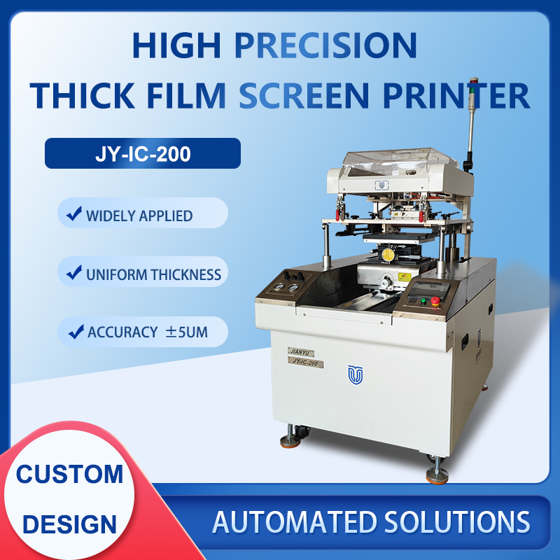
●Maximum printing area: 200 × 200 mm
●Suitable for printing on ceramic antennas, ceramic substrates, PCBs, and electronic components
●This equipment holds 1 invention patent and 5 utility model patents.
4.Application Scenarios of Ceramic Antennas
In recent years, with the continuous upgrading of wireless communication technology, ceramic antennas have been widely used in various industries.
Surveying and Mapping 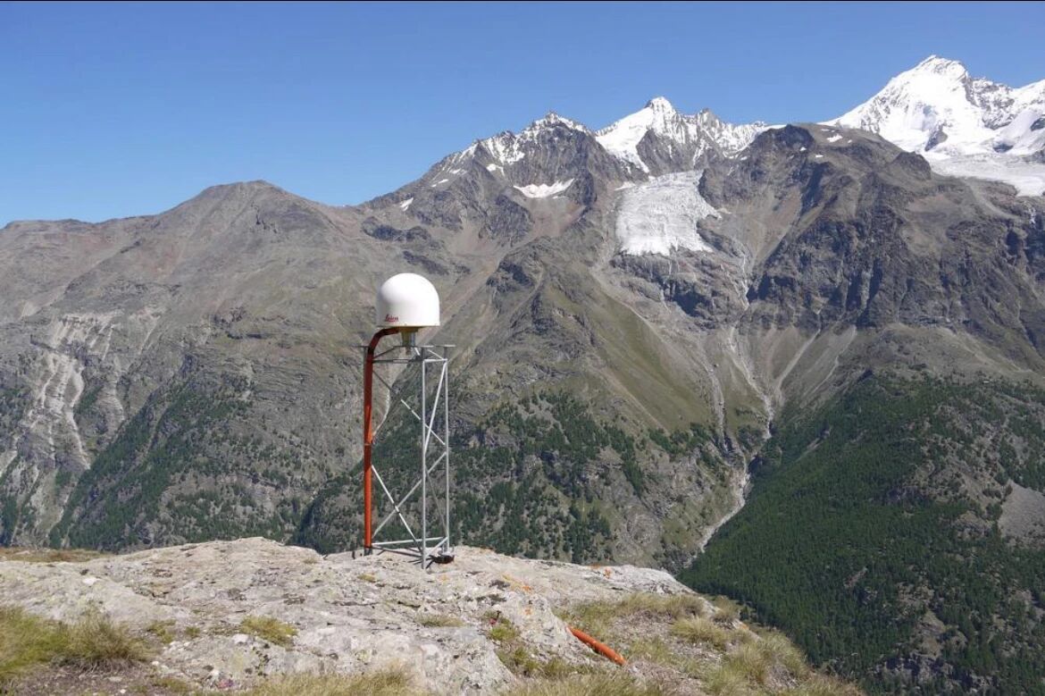
Disaster Monitoring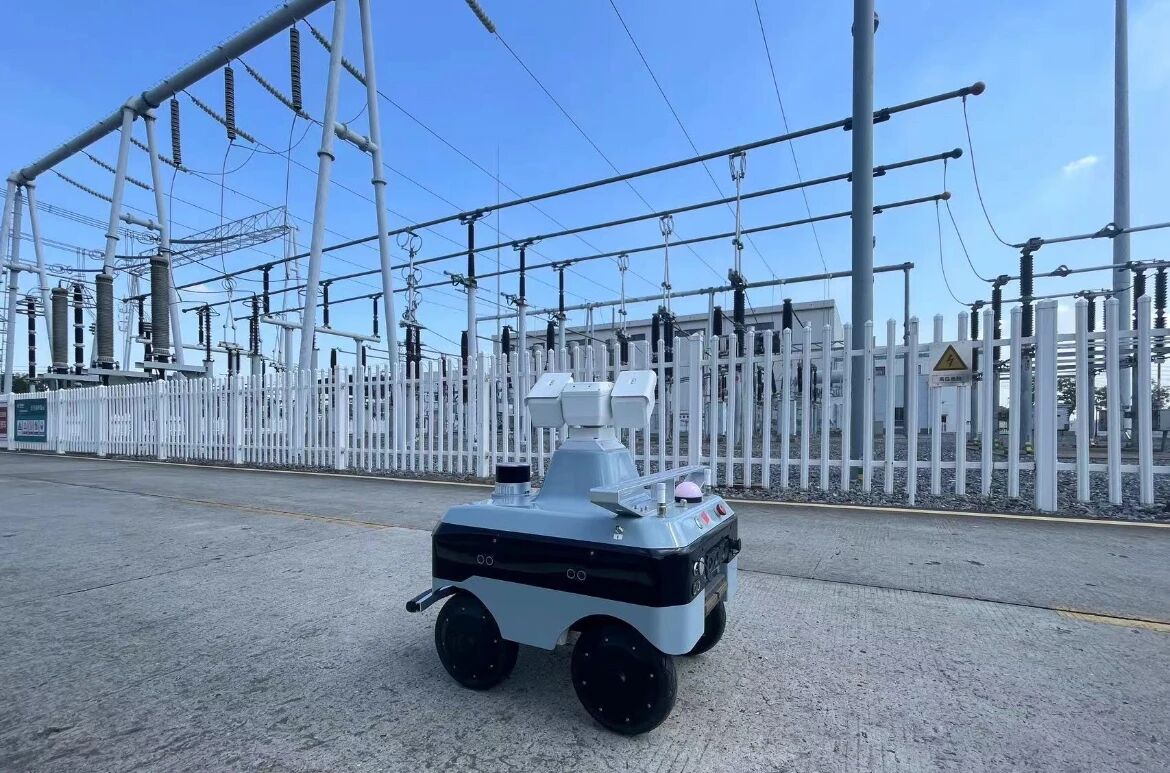
Robotics 
Precision Agriculture
UAV 
Smart Vehicle
Ceramic Antenna Application Scenarios Image Source: Internet
5.Conclusion
Behind a tiny ceramic antenna lies the convergence of wireless communication, materials science, and precision manufacturing technologies. From ground layers to radiating patches, from single-layer structures to multilayer LTCC, and from conductive pastes to high-temperature sintering, every step relies on the support of high-precision thick film printing processes.
In the future, with the development of emerging industries such as 5G, smart vehicles, the low-altitude economy, and the Internet of Things, ceramic antennas will play an even more important role in the field of wireless communication. Jianyu Screen Printing will also continue to deepen its expertise in high-precision thick film printing technology, providing stable, efficient, and accurate equipment solutions to help customers achieve higher-quality manufacturing of ceramic antennas and electronic ceramic products.