Against the global shift to greener, low‑carbon energy, photovoltaic (PV) power stands out as one of the most promising clean energy solutions. A PV cell combines materials science, precision engineering, and automation. Among its core processes, thick‑film screen printing is vital for electrode fabrication and conductive pattern formation. High‑precision printing equipment not only determines production throughput but also directly influences conversion efficiency and product uniformity.
1.What is a photovoltaic cell?
A photovoltaic cell, also known as a solar cell, is a semiconductor device that converts sunlight directly into electricity through the photovoltaic effect. Its core material is typically a silicon wafer; when sunlight strikes the cell surface, an electric current is generated, enabling the conversion of light energy into electrical energy.
PV cells are widely used in renewable energy generation, distributed PV systems, energy storage, new energy vehicles, and many other fields. They are the most essential component of any photovoltaic power system.
Depending on the material and technological route, PV cells are mainly classified into crystalline silicon solar cells, thin‑film solar cells, and next‑generation high‑efficiency solar cells. Among these, crystalline silicon cells remain the most widely adopted technology in the market today.
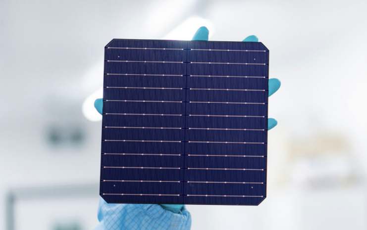
Image source: Internet
Image source: PV Technology WeChat Official Account
Throughout this printing process, the pattern must be complete, lines clear, thickness uniform, and alignment precise—ensuring excellent electrical conductivity and conversion efficiency in the final PV cell.4. The role of thick‑film printing equipment in PV manufacturingDuring electrode preparation, thick‑film screen printing equipment is the key enabler of pattern accuracy and consistency. Control over electrode line width, paste transfer stability, and registration accuracy all directly affect cell efficiency and yield.High‑precision thick‑film screen printing systems typically require vision‑alignment systems, stable motion control, and precise squeegee pressure regulation to ensure that materials like silver paste are uniformly and accurately transferred onto the wafer surface, forming high‑quality electrode structures.
Recommended equipment: JY‑IC‑200A‑CCD
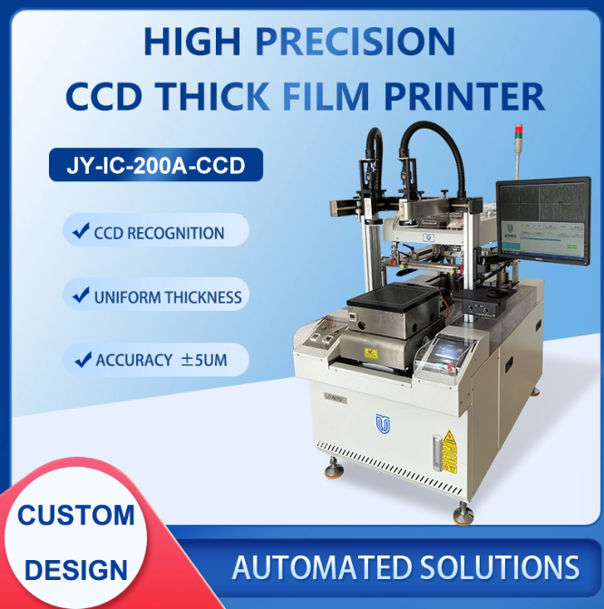
- Maximum printing area: 200 × 200 mm
- CCD vision system improves loading accuracy and increases work efficiency
- Suitable for solar cells, ceramic substrates, PCBs, and electronic component printing
- This model is protected by 1 invention patent and 5 utility model patents
5. ConclusionAs high‑efficiency PV cell technologies continue to evolve, the photovoltaic industry is moving toward higher conversion efficiencies, lower manufacturing costs, and more intelligent production. As one of the core processes in PV cell fabrication, thick‑film screen printing will keep playing a vital role in enhancing product performance, manufacturing efficiency, and consistency.As a manufacturer of high‑precision thick‑film screen printing equipment, JYUTEC will continue to deepen its expertise in precision printing technology, continuously improving equipment performance and process solutions. We are committed to providing stable, efficient printing solutions for the photovoltaic, new‑energy electronics, and advanced manufacturing sectors, contributing to the high‑quality development of the green energy industry through precision engineering.